Semiconductor image sensor
Turning light into electrical signals
Contents
- 1Photosensitive silicon array
- 2Transfer along columns
- 3Serial readout register
- 4Output stage
- 5Analogue output signal
A semiconductor image sensor converts a pattern of light into electrical signals, using architectures developed from the early 1960s. In the CCD variant, charges collected in silicon are transferred to an analogue output whose measurement can then be digitised.
What it is
An electronic image sensor turns a pattern of light into electrical signals. In a CCD, or charge-coupled device, photosensitive sites collect charges representing the illumination received during an exposure. Each measurement’s position in the array allows the spatial pattern to be reconstructed.
MOS and CCD families organise readout differently. In a passive-pixel MOS sensor, a transistor selects a photodiode and passes its signal to a shared circuit; an active pixel adds local amplification. In a CCD, packets of charge travel through the semiconductor to the output. These arrangements separate the collection of light from the way its electrical measurement is extracted.
Light absorbed in silicon can create charge carriers. Electric fields collect the useful electrons. The sensor retains a local measurement; the lens that forms the image and the system that records it perform other tasks.
The quantities produced by a CCD are initially analogue. An analogue-to-digital converter turns their measurement into numerical values. Sensing, readout and digitisation are successive functions in an imaging chain. An electrical image signal can also be used for analogue video.
How it works
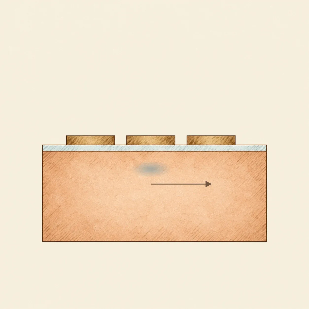 Gate voltages move the electrical storage regions; the silicon itself stays still.
Electrodes insulated from the silicon by an oxide create potential wells. These are regions in which an electric field can hold charge, rather than little containers hollowed out of the crystal.
Charges accumulate during the exposure. In a simple array architecture, controlled electrode voltages then shift the packets down columns into a serial register. This register presents them one after another to the output stage, where they can be measured as a voltage. The readout sequence preserves the original position associated with each measurement.
The response has limits. A site can saturate; dark current adds charge even without illumination, and readout introduces noise. Pixel count alone therefore cannot describe image quality.
 A filter mosaic selects colours before the charges are collected.
Colour filters separate parts of the spectrum. With a filter mosaic, each photosite receives only part of the colour information. Processing combines neighbouring measurements to reconstruct the colours of the image.
In a full-frame CCD, the same surface receives light and subsequently transfers charge. Readout takes place while illumination is interrupted, for example with an external shutter closed, to limit signal added during transfer. Other architectures provide a separate storage area or shielded registers alongside the photosites. The choice changes how exposure and readout can follow one another.
How to do it
Manufacturing a CCD uses a highly pure silicon wafer, doped regions, insulating layers, electrodes and metal connections. Cleanroom microfabrication processes form the patterns. In an aluminium-metallised variant, this metal provides connections and shields areas that must be kept dark. Packaging then allows the chip to be used without exposing its fragile layers.
To explore readout, draw a grid on paper and put counters in its cells to represent different illumination levels. Start with the bottom row, move it into the readout strip, then shift its counters towards the counting cell on the right; read the rightmost cell first. Repeat for the remaining rows, working upwards. Record the results in sequence and place those numbers in an identical grid.
Do not strip, heat or break a chip to look for pixels.
History and evolution
In the early 1960s, Paul Weimer at RCA explored sensors made with thin-film transistors on glass. In 1963, S. R. Morrison at Honeywell presented devices with diffused diode junctions in silicon, including a scanner and a light-spot position detector. IBM reported the scanistor in 1964: its junctions supplied a signal related to local illumination. These devices preceded intentional accumulation of charge within the pixels.
Solid-state sensors existed before the CCD. In 1967, Gene Weckler studied the integration of photodiode signals. In 1968, Peter Noble described silicon detector arrays with controlled readout and amplification within the pixel.
At Bell Labs in 1969, Willard Boyle and George Smith conceived the CCD charge-transfer principle while working on memory devices. Their initial notes are dated 8 September. Publications in 1970 and subsequent work by Michael Tompsett and his colleagues led to imaging applications.
CMOS active-pixel sensors use a different readout arrangement. Amplification takes place locally within the pixel, with rows and columns addressed for readout. In the early 1990s, Eric Fossum’s team at JPL developed this approach for compact cameras. Local charge transfers within some CMOS pixels do not turn the array into a CCD. Both families use photoelectric conversion, with different architectures.