Integrated circuit
Components and connections on a chip
Contents
- 1Insulating package of the NE555 timer
- 2Package orientation notch
- 3Positive supply pin
- 4Ground pin
- 5Output pin
Loading the figure…
An integrated circuit, or microchip, brings components and their connections together on a semiconductor. Werner Jacobi filed a patent in 1949 describing several amplifier stages on one semiconductor. Counters developed in the 1950s, followed by the work of Kilby and Noyce, explored different forms of integration.
What it is
An integrated circuit contains electronic components on a small piece of semiconductor, together with the connections that let them perform a shared task. A chip can process signals, store information or provide timing. Its job depends on the components it contains and the way they are connected. Processors are one application among many. Making these elements together reduces the number of separate parts to assemble and the connections needed between them.
The package protects the chip and provides terminals large enough to connect it to equipment. The NE555 is a current commercial timer, available as the NE555P in an eight-pin PDIP package. It is a later device than Kilby’s experimental circuit. With external resistors and capacitors, the timer can produce a timed interval or an oscillation. The semiconductor chip inside and its protective outer package are distinct parts of the finished component.
How it works
Components are formed in selected regions of the semiconductor and connected according to a planned layout. In Robert Noyce’s proposed planar structure, metal tracks above an oxide layer link the components. The oxide keeps the conductors apart from the silicon where current must not pass between them. Openings provide contacts at the intended locations. These interconnections give neighbouring elements a common electrical function; putting components on the same piece of material also requires a way to connect and isolate them.
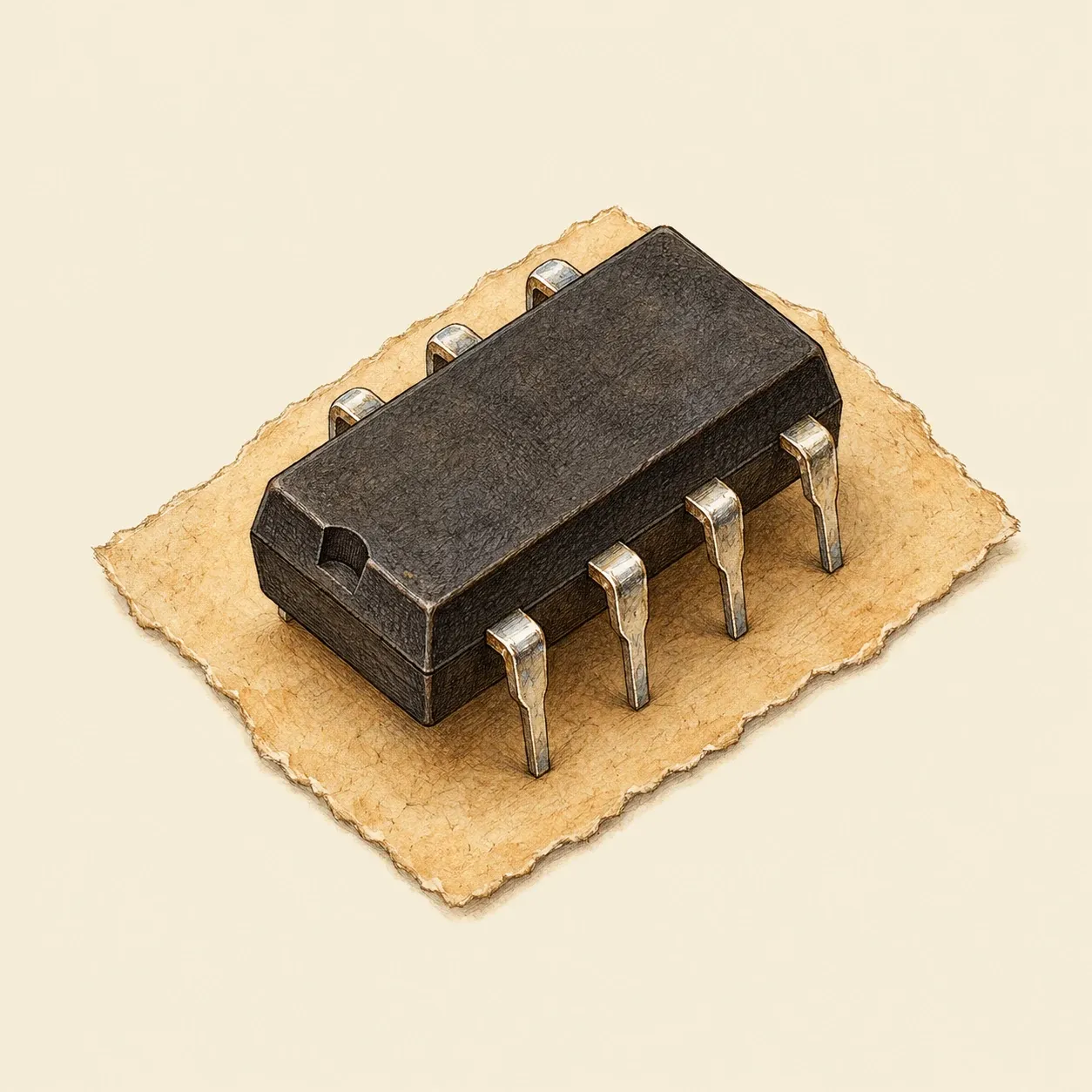 The notch establishes the orientation of the eight-pin package when reading its pinout.
On the PDIP version of the NE555, pin eight takes the positive supply, pin one is ground and pin three provides the output. Inside the chip, comparators monitor voltages and a latch holds the state that controls the output. In timing circuits, an external capacitor charges or discharges. Changes in its voltage determine when the state switches. The resulting delay therefore depends on components outside the chip as well as the circuitry within it.
A closed package conceals the size of the chip and the number of components inside. Devices with the same outline can perform different jobs and have different pin assignments. Identify a real component by its part number, then consult the corresponding manufacturer’s documentation. An unsuitable supply or an electrostatic discharge can damage a chip. Electrical limits belong to the particular model for which they are specified.
How to do it
A silicon wafer receives successive conducting, insulating or semiconducting layers. Photolithography transfers patterns into a light-sensitive resist. The patterned regions allow selected areas to be treated while others remain protected. Repeated operations, with checks along the way, form the circuit structures and the connections between them.
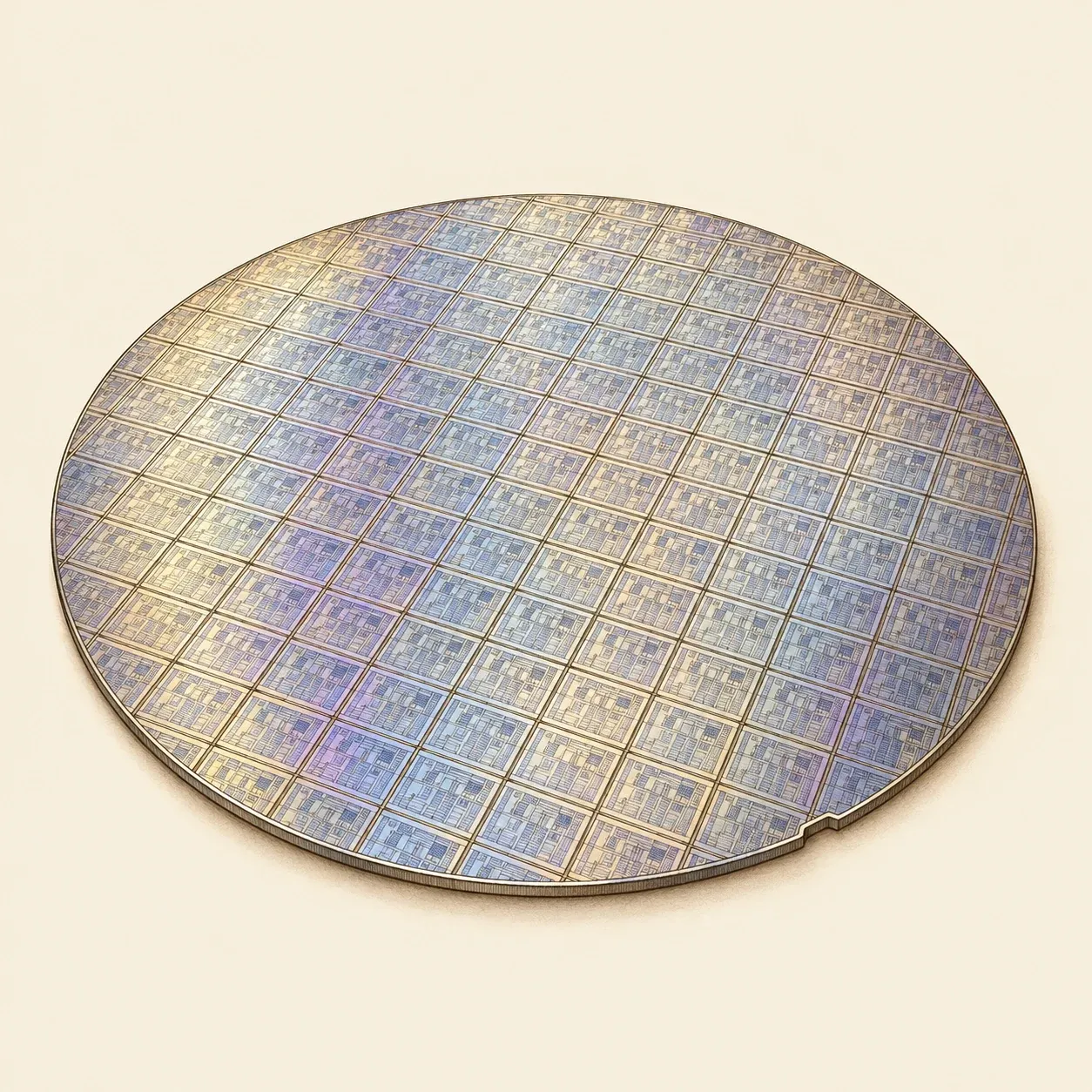 Many circuits are made on a wafer before it is divided into individual chips.
Some treatments change the semiconductor’s properties locally; others add or remove material. Measurements check the results during manufacture. Once the patterns are complete, the wafer is cut into individual dies, which are then protected in packages. Cleanliness matters throughout this work. A particle in the wrong place can make a circuit unusable.
These processes require industrial facilities equipped to handle their chemicals and machinery. Keep a component’s package intact: do not open, strip, heat or grind it. For an unpowered examination, look at the outside of the package and compare its orientation with the manufacturer’s drawing. An enlarged paper diagram lets you follow the order of the pins without handling the internal connections. Leave the component disconnected from any power supply.
History and evolution
In 1949, Werner Jacobi filed a patent describing several amplifier stages on a single semiconductor, with coupling between the stages. The patent was published in 1952. That year, Geoffrey Dummer publicly proposed a solid electronic block without connecting wires.
Rick Dill later recalled making a multistate counter at IBM in the summer of 1954, under Joe Logue’s direction. Arthur D’Asaro recalled a Bell Labs counter becoming operational in late 1955, with several switches in one piece of silicon. These accounts describe specialised integrated functions.
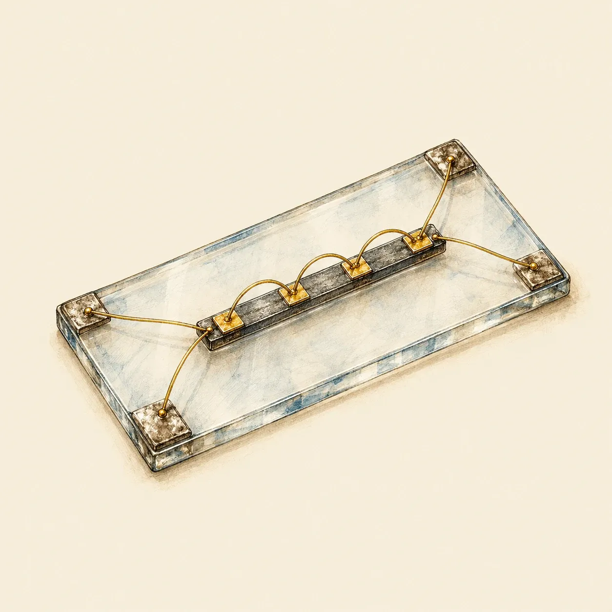 Germanium elements joined by fine gold wires: such connections made mass production difficult.
On 12 September 1958 at Texas Instruments, Jack Kilby demonstrated an oscillator made with germanium elements joined by fine gold wires. His work showed that a semiconductor could provide active and passive elements. The wire connections, however, made mass production difficult.
Kilby filed his patent application on 6 February 1959. At Fairchild, Robert Noyce drew on Jean Hoerni’s planar process and proposed metal connections over the silicon’s protective oxide. He filed on 30 July 1959. A Fairchild team made working monolithic circuits in May 1960. Isolating the components from one another was another problem that had to be solved.
Texas Instruments marketed an early device in 1960, still constrained by wire connections. The planar approach subsequently enabled mass production and remains the basis of integrated-circuit manufacture. Kilby and Noyce are recognised as co-inventors for their different contributions. Chips became components in computers and many other kinds of equipment, with functions extending well beyond those of a processor.