Flash memory
Stored charge and erasure in groups
Contents
- 1Control gate
- 2Insulator around the floating gate
- 3Floating gate
- 4Source
- 5Channel in silicon
- 6Drain
Flash memory retains data when power is removed. It is programmed electrically and erased in groups of cells.
What it is
Flash is nonvolatile electronic memory: information remains when power is switched off. It belongs to the electrically erasable memory family, EEPROM. Conventional EEPROM allows small units to be changed separately. Flash saves cell area by arranging erasure over groups of cells. Reading, programming and erasing are separate operations with different effects on the stored information.
A cell is the element that holds information. A chip brings many cells together with selection and read circuits. A memory card, USB drive or SSD adds an interface and control circuitry. A saved file depends on the complete system.
How it works
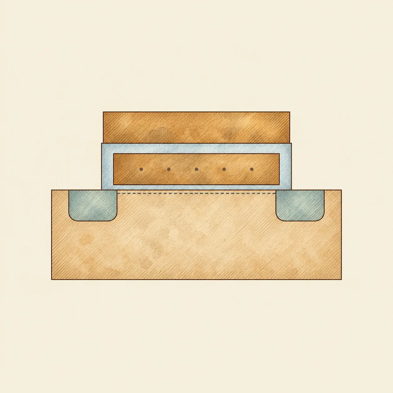 The floating gate holds charge without a conducting connection to the outside.
In a planar floating-gate cell, a conducting region is surrounded by insulation between the silicon channel and the control gate. Programming can inject electrons accelerated in the channel into the floating gate. Erasure can remove them by tunneling through a thin oxide layer under a strong electric field. The retained charge changes the voltage needed to make the transistor conduct. A read circuit applies controlled conditions and distinguishes states through the resulting current. No mechanical part moves during storage or reading.
NOR and NAND describe the connections between cells. NOR cells form parallel branches connected to a bit line. This suits reading individual addresses and, in suitable memory systems, executing program code directly. NAND connects cells in series strings. Page access and a denser layout suit data storage. Although the names come from logic gates, a flash array has selection, storage and reading functions beyond an ordinary logic gate.
Multilevel cells distinguish more charge states to encode several bits. Programming and erasure stress the insulation, so endurance and retention have limits. Controllers can correct errors and distribute writes across the memory. Holding information without power does not guarantee permanent preservation. A retention period or cycle limit must be specified for a particular device and its conditions of use.
How to do it
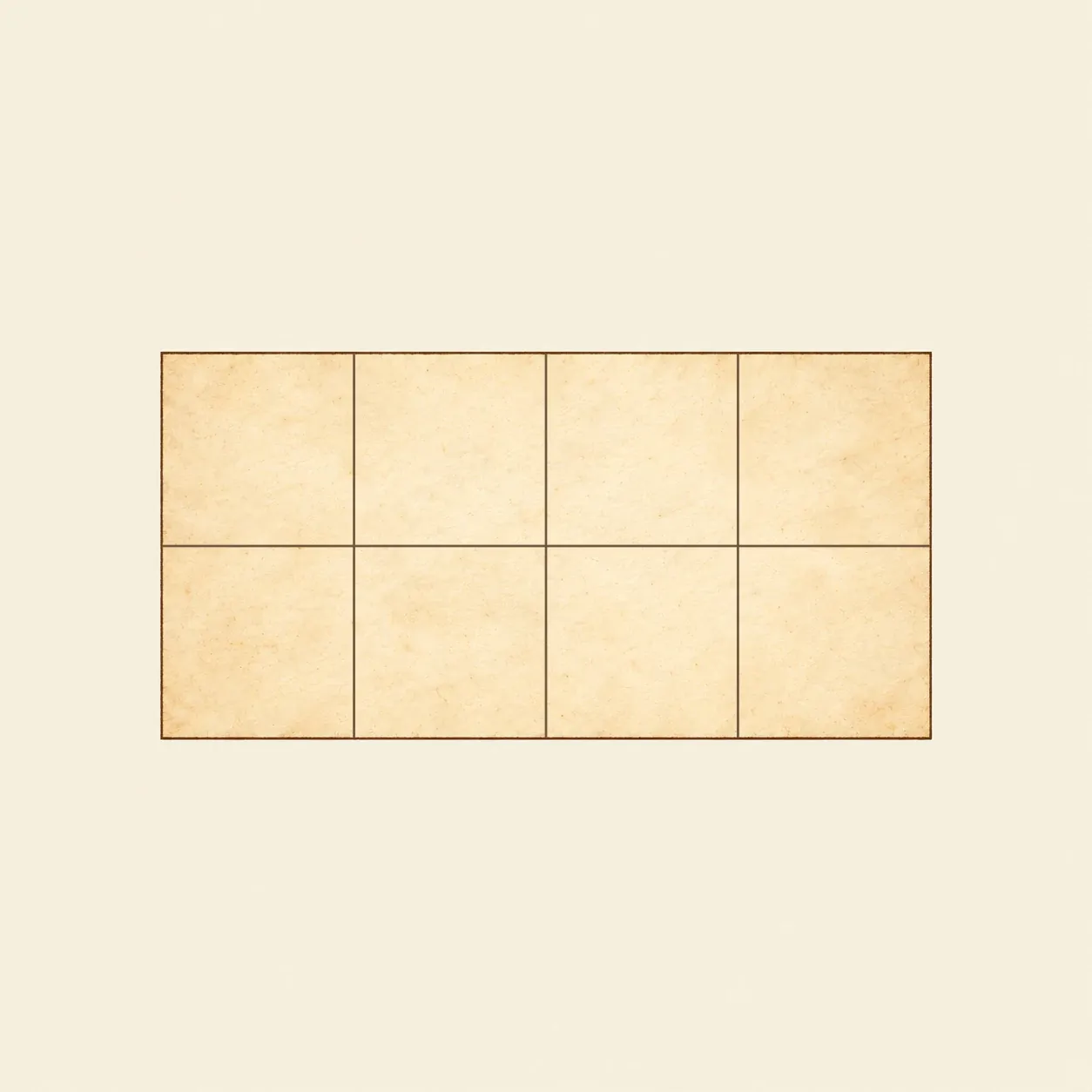 All squares in the paper model belong to the same erase block.
Manufacture uses integrated-circuit processes: patterns in silicon, insulating and conducting layers, connections, testing and packaging. In one planar NMOS process, the silicon body is doped with boron and the source and drain regions with phosphorus. Industrial processes involve reactive chemicals and specialized equipment. Keep chips sealed; do not strip or heat them. The following activity uses paper alone.
Draw a block with two four-bit words, initially 1111 and 1111. In this binary model, programming can only change a 1 to a 0. Erasing restores the whole block to 1. Write 1010 in the first word and 0011 in the second.
Now try changing the first word to 1110. That would require a 0 to become a 1, which programming alone cannot do. Copy both words to a working sheet, change the first, erase all eight squares together and write back 1110 and 0011. The second word survives because you kept a copy. Erasing without that copy would lose it.
History and evolution
Charge storage memories came before flash. Kahng and Sze published their floating-gate work in 1967. Intel introduced Frohman’s EPROM in 1971; it was programmed electrically and erased with ultraviolet light. EEPROM developments subsequently brought electrical erasure with finer selection of cells. In 1979, Horiuchi and Katto described FCAT, another floating-gate device that could be programmed and erased electrically.
In 1980, Kupec and colleagues described a triple-polysilicon EEPROM with one transistor per bit. Masuoka and Iizuka’s patent application for a cell with an erase gate claims Japanese priorities of 20 December 1980; the US application followed in 1981 and became patent US4531203 in 1985. Harari later placed Kupec’s cell among flash prior art and described Masuoka and Iizuka’s cell as an improvement.
Masuoka and his Toshiba team sought a more compact cell. He described their NOR flash cell at the 1984 IEDM. This research and presentation preceded large-scale commercial manufacture. Other teams, including engineers at Intel, developed NOR structures suitable for production.
Toshiba announced NAND in 1987. In his testimony published by the IEEE, Masuoka says that tests that year verified programming, reading and erasure; a 4 Mbit NAND prototype was developed in 1988 and presented at ISSCC in 1989. Kioxia, the successor to that memory business, dates commercialization of a 4 Mbit NAND to 1991. Memory cards and SSDs later formed complete storage systems around flash cells. Multilevel operation and three-dimensional structures extended the technology further.